Search result


Finally... Samsung has officially started rolling out the impending Jelly Bean update for Samsung Galaxy S II. The update is currently available in Spain but we shall see the update soon in many other countries as well.
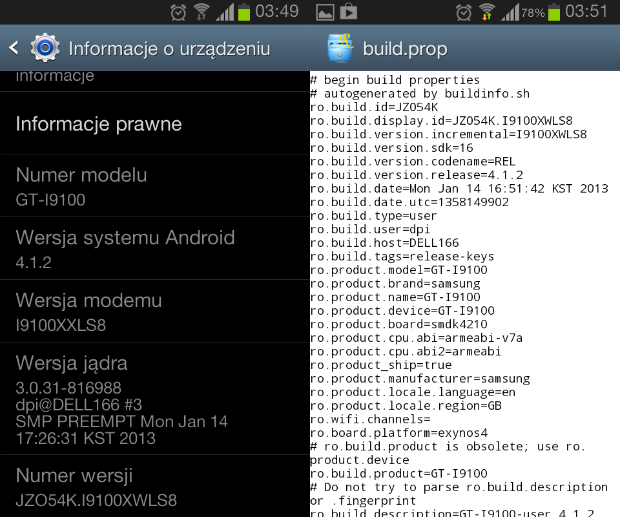
The XWLS8 update is different from the ROM that was leaked months ago but runs Android 4.1.2 with a recent January 2013 build date.
The Jelly Bean update will bring the new TouchWiz Nature UI to the GS II. Until now, the handset was stuck with Samsung's old version of TouchWiz, which was much less appealing, and also brings lots of performance improvements, expandable and actionable notification panel, and Google Now.
Enhancements of the Jelly Bean update:
- Buttery Smooth Performance & Great Stability (Thanks to Project Butter)
- Full User Interface Revamp (Same UI as of the Galaxy S III and Galaxy Note II)
- TouchWiz Nature UX
- Samsung's S Cloud services
- Improved Camera features
- New Lockscreen With Many Customization Options
- New Features like Direct Call, Smart Stay and Pop-up Play
- New Widgets (From Galaxy S III)
- 2 Home screen modes
- New Notification bar With More Notification Toggles
- Google Now
Source: PhoneArena

Check out this Woot deal for the Samsung Galaxy Note 10.1. The tablet is being sold in refurbished condition starting at $379.99 for a 16GB model in white or deep grey. The 32GB version is priced at $419.99.
The Samsung GALAXY Note 10.1 is outfitted with the functionality and precision of a pen and paper on a 10.1-inch-large-display.
Featuring an intuitive user experience and armed with superior hardware performance, GALAXY Note 10.1 is designed to simplify idea capturing, information access, and multi-tasking, making each easier and faster.
Hoot Link to buy
Check below video for Hands On video on the Galaxy Note 10.1

Samsung Electronics, the world leader in advanced memory technology, today announced that it has begun mass producing the industry's first three-dimensional (3D) vertical NAND (V-NAND) flash memory, which breaks through the current scaling limit for existing NAND flash technology. The new 3D V-NAND will be used for a wide range of consumer electronics and enterprise applications, including embedded NAND storage and solid state drives (SSDs).
Samsung's new V-NAND offers a 128Gb density in a single chip, utilizing the company's proprietary vertical cell structure based on 3D charge trap flash (CTF) technology and vertical interconnect process technology to link the 3D cell array. By applying both of these technologies, Samsung's 3D V-NAND is able to provide over twice the scaling of 20nm-class planar NAND flash.
See press release below:
SEOUL, South Korea-(BUSINESS WIRE)-Samsung Electronics Co., Ltd., the world leader in advanced memory technology, today announced that it has begun mass producing the industry's first three-dimensional (3D) Vertical NAND (V-NAND) flash memory, which breaks through the current scaling limit for existing NAND flash technology. Achieving gains in performance and area ratio, the new 3D V-NAND will be used for a wide range of consumer electronics and enterprise applications, including embedded NAND storage and solid state drives (SSDs).
"Following the world's first mass production of 3D Vertical NAND, we will continue to introduce 3D V-NAND products with improved performance and higher density, which will contribute to further growth of the global memory industry."
Samsung's new V-NAND offers a 128 gigabit (Gb) density in a single chip, utilizing the company's proprietary vertical cell structure based on 3D Charge Trap Flash (CTF) technology and vertical interconnect process technology to link the 3D cell array. By applying both of these technologies, Samsung's 3D V-NAND is able to provide over twice the scaling of 20nm-class* planar NAND flash.
"The new 3D V-NAND flash technology is the result of our employees' years of efforts to push beyond conventional ways of thinking and pursue much more innovative approaches in overcoming limitations in the design of memory semiconductor technology," said Jeong-Hyuk Choi, senior vice president, flash product & technology, Samsung Electronics. "Following the world's first mass production of 3D Vertical NAND, we will continue to introduce 3D V-NAND products with improved performance and higher density, which will contribute to further growth of the global memory industry."
For the past 40 years, conventional flash memory has been based on planar structures that make use of floating gates. As manufacturing process technology has proceeded to the 10nm-class* and beyond, concern for a scaling limit arose, due to the cell-to-cell interference that causes a trade-off in the reliability of NAND flash products. This also led to added development time and costs.
Samsung's new V-NAND solves such technical challenges by achieving new levels of innovation in circuits, structure and the manufacturing process through which a vertical stacking of planar cell layers for a new 3D structure has been successfully developed. To do this, Samsung revamped its CTF architecture, which was first developed in 2006. In Samsung's CTF-based NAND flash architecture, an electric charge is temporarily placed in a holding chamber of the non-conductive layer of flash that is composed of silicon nitride (SiN), instead of using a floating gate to prevent interference between neighboring cells.
By making this CTF layer three-dimensional, the reliability and speed of the NAND memory have improved sharply. The new 3D V-NAND shows not only an increase of a minimum of 2X to a maximum 10X higher reliability, but also twice the write performance over conventional 10nm-class floating gate NAND flash memory.
Also, one of the most important technological achievements of the new Samsung V-NAND is that the company's proprietary vertical interconnect process technology can stack as many as 24 cell layers vertically, using special etching technology that connects the layers electronically by punching holes from the highest layer to the bottom. With the new vertical structure, Samsung can enable higher density NAND flash memory products by increasing the 3D cell layers without having to continue planar scaling, which has become incredibly difficult to achieve.
After nearly 10 years of research on 3D Vertical NAND, Samsung now has more than 300 patent-pending 3D memory technologies worldwide. With the industry's first completely functional 3D Vertical NAND memory, Samsung has strengthened its competitiveness in the memory industry as well as set the foundation for more advanced products including one terabit (Tb) NAND flash, while setting a faster pace for industry growth.
According to IHS iSuppli, the global NAND flash memory market is expected to reach approximately US $30.8 billion in revenues by the end of 2016, from approximately US $23.6 billion in 2013 with a CAGR of 11 percent, in leading growth of the entire memory industry.

Our Mission is Keeping you updated with Latest Android News and Updates as it Happens!

© 2023 YouMobile Inc. All rights reserved